TECH
Innovative Uses for Patterned Silicon Wafers in Technology
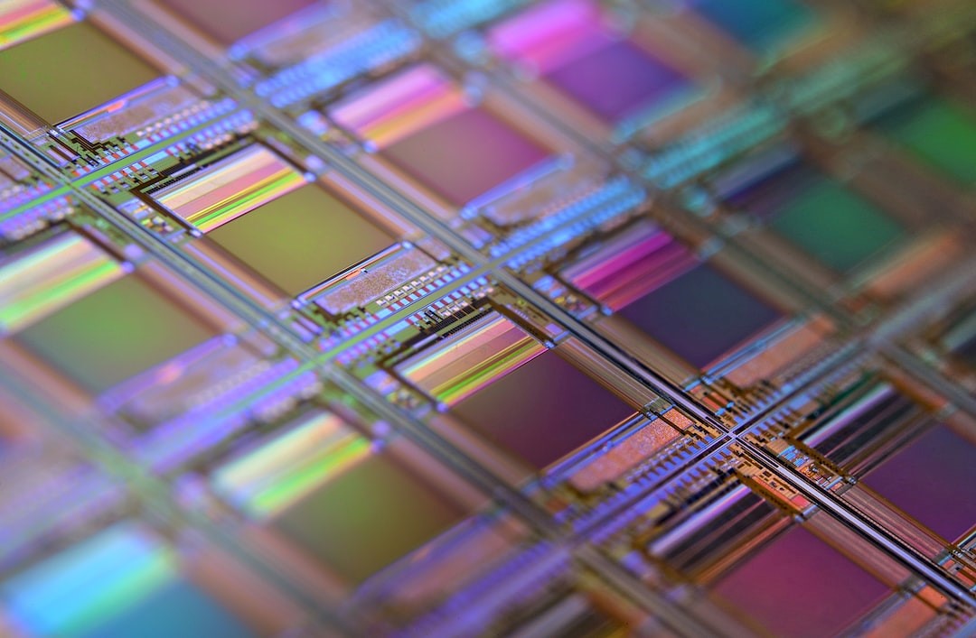
Patterned silicon wafers shape the core of today’s fast-moving tech world. They form the base for devices that run faster, think smarter, and connect deeper. Behind every breakthrough, they quietly set the pace for what’s next.
Each pattern tells a story of precision and progress. As designs grow smaller, their impact grows larger. The future of technology begins right here, layer by layer, on every silicon surface.
In this blog, we will discuss innovative applications of patterned silicon wafers in technology. Keep reading.
How Patterned Silicon Wafers Power Next-Generation Microelectronics
Patterned silicon wafers form the base of modern microelectronics. They let circuits fit into smaller spaces while keeping everything stable. Through semiconductor lithography, fine designs are made that help devices work the way they should.
Microelectronic engineering uses these designs to keep systems simple but powerful. When signals move through clean paths, the devices stay steady. This balance makes every product last longer and perform better.
The rise of digital tools depends on structure and control. Patterned wafers make both possible by keeping everything in order. That is how new ideas in electronics become real and ready to use.
Enabling Faster and Smaller Semiconductor Devices
Nanofabrication technology allows smaller, quicker devices to take shape. Patterned silicon wafers make this possible by holding designs that control signal flow. Each small pattern has a big effect on speed and strength.
Smaller chips can now do more work with less space. As engineers build faster tools, they rely on the structure inside the wafer. That structure keeps things running smoothly and steadily.
The world of semiconductors grows with every new pattern. Each wafer design pushes limits while keeping devices safe. This step keeps the future of small and strong technology moving forward.
Boosting Energy Efficiency in High-Performance Computing Systems
Patterned silicon wafers help computers stay cool and steady. By spreading energy evenly, they stop systems from getting too hot. This design supports fast work without waste.
High-performance systems rely on microelectronic engineering to stay balanced. Each wafer keeps energy paths clean and short. That is how machines stay active longer without slowing down.
With new semiconductor lithography, even small changes make a big difference. Energy moves faster and safer through better patterns. This control helps big systems save power while staying strong.
The Role of Patterned Wafers in Advanced Sensor Technologies
Patterned silicon wafers are the center of modern sensors. They help read light, heat, and sound with clear results. Each layer inside the wafer helps sensors stay sharp.
Nanofabrication technology lets sensors catch even tiny changes. This means machines can see, hear, and feel better than before. That power shapes safer cars, cleaner labs, and smarter tools.
Wafer-level packaging keeps these sensors safe and small. It locks their parts together while keeping signals clear. Each pattern inside the wafer helps sensors work better everywhere.
Driving Innovation in MEMS and Nanoelectromechanical Systems
MEMS devices are tiny systems that move and measure with care. Patterned silicon wafers are what make them possible. They guide every small motion that helps machines think and act.
Through semiconductor lithography, patterns are built with exact lines. Each pattern lets MEMS parts move without breaking. This makes them useful in health, science, and engineering.
Nanofabrication technology gives engineers the power to build at a tiny scale. Patterned wafers let parts fit tightly together and stay stable. That keeps MEMS and Nanoelectromechanical Systems growing stronger and smaller.
Enhancing Signal Integrity in Communication Devices
In communication systems, clean signals are key. Patterned silicon wafers keep electrical paths straight and free from noise. This helps devices send messages fast and clear.
Microelectronic engineering uses wafer design to reduce weak spots. Each smooth surface supports steady signal flow. That is why phones, radios, and routers work without delay.
Wafer-level packaging protects parts from dust and damage. It also keeps signals inside where they belong. Patterned wafers make sure every message gets through.
Paving the Way for AI and Quantum Computing Hardware
Artificial intelligence depends on fast and exact hardware. Patterned silicon wafers shape that foundation with perfect control. Each pattern helps computers learn and process faster.
Quantum systems need balance and order to work properly. Through nanofabrication technology, wafers hold that order in place. This makes sure data moves safely inside complex circuits.
Semiconductor lithography builds designs that match quantum rules. It gives systems the power to think beyond what humans can. Patterned wafers are the silent base of that growth.
Improving Thermal Management in Compact Electronic Components
Small devices make a lot of heat. Patterned silicon wafers help move that heat away. This keeps parts safe and helps everything last longer.
Microelectronic engineering builds wafers that spread warmth evenly. That keeps chips from burning out or slowing down. Small changes in pattern make a big difference in safety.
Nanofabrication technology lets engineers shape heat paths with care. This keeps even tiny tools cool and steady. Patterned wafers protect both speed and life inside compact devices.
Expanding the Capabilities of Photonic and Optoelectronic Devices
Light-based devices rely on control and order. Patterned silicon wafers guide light through every layer. This helps make cameras, sensors, and lasers work better.
Through semiconductor lithography, light moves cleanly without loss. That makes pictures clearer and signals stronger. Each pattern acts like a map for every beam.
Wafer-level packaging lets parts stay together without blocking light. It keeps systems clear and ready to perform. Patterned wafers make sure light stays useful in every step.
Streamlining Semiconductor Fabrication for Higher Yields
Patterned silicon wafers make chip building faster and cleaner. They help lower waste and keep shapes uniform. This leads to stronger production lines with steady output.
Microelectronic engineering supports these patterns with tight rules. This helps factories make more chips in less time. The goal is always quality and repeatable success.
The use of customized patterned silicon wafers makes building smarter and safer. It joins modern semiconductor lithography with solid nanofabrication technology. This teamwork raises quality and helps each new product reach its full value.
The Future Ahead with Patterned Silicon Wafers
Patterned Silicon Wafers continue to shape how the world connects, learns, and creates. They form the quiet strength behind every major step in modern innovation. Each design helps build faster, smarter, and more reliable technology that keeps industries moving forward.
As new ideas rise, these wafers will guide the way. They remain the foundation where progress begins. Explore how precision in every layer can lead to your next breakthrough.

-
 TECH3 months ago
Modern Applications of Aerospace Fasteners
-
 TECH2 months ago
The Evolution and Future of Bearing Technology
-

 GUIDE2 months ago
Creek-to-Ridge Design: Effective Water Management for Regenerative Landscapes
-

 TECH2 months ago
How Automation is Revolutionizing Industrial Brazing: Trends, Technologies, and Industry Leaders